Information
Overview
CoWoS-S (redraw needed)
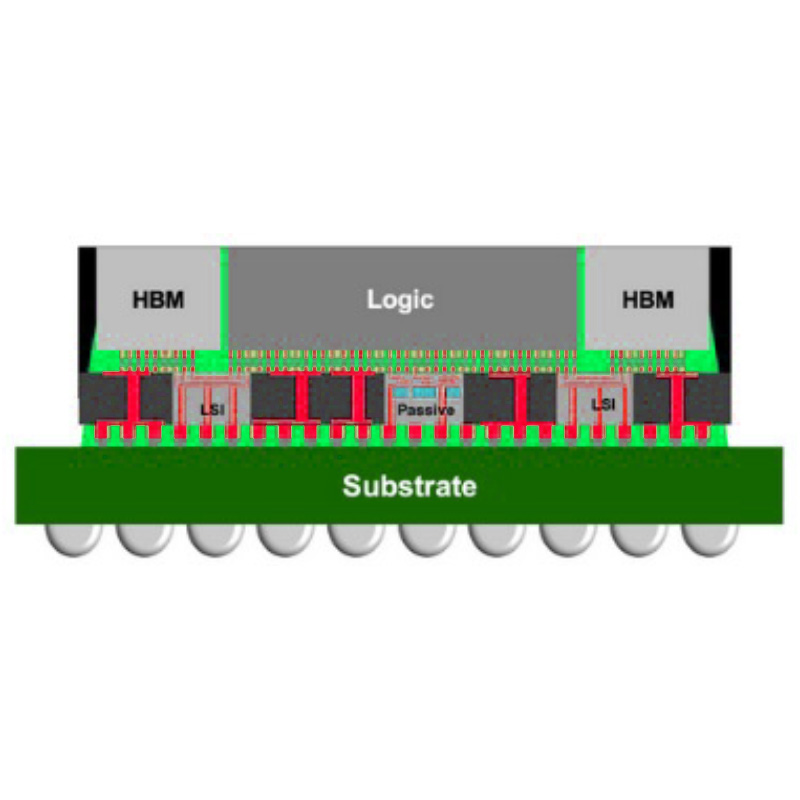
CoWoS-R (redraw needed)
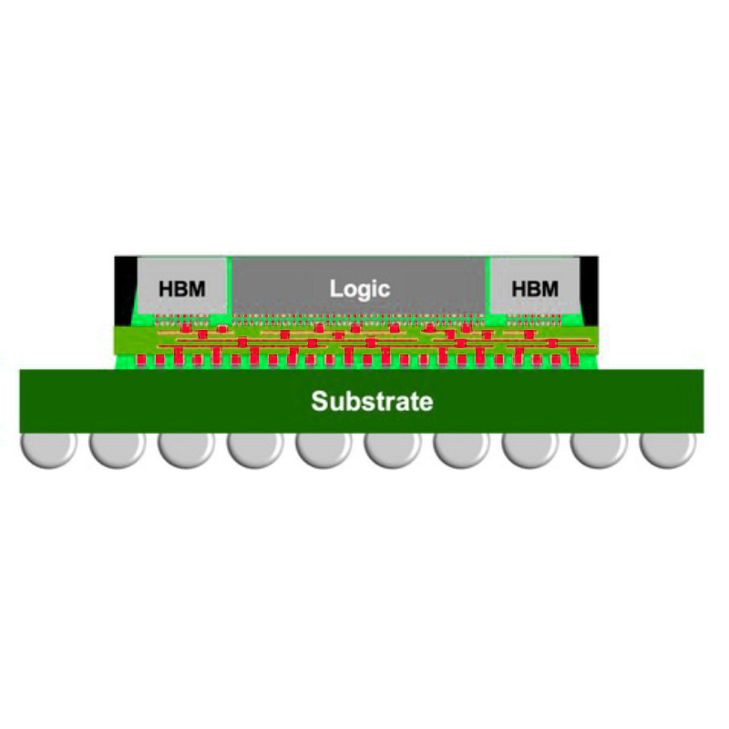
CoWoS-L (redraw needed)
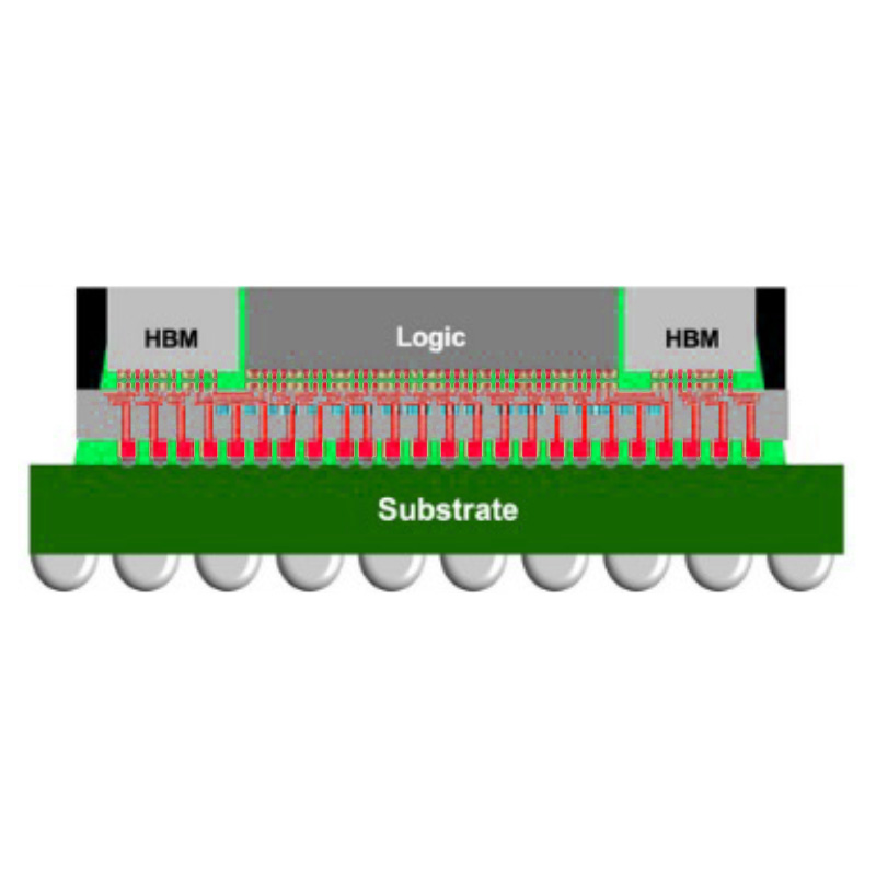
InFO-oS (redraw needed)
TSMC-SoIC (redraw needed)
System-on-Wafer (SoW) (redraw needed)
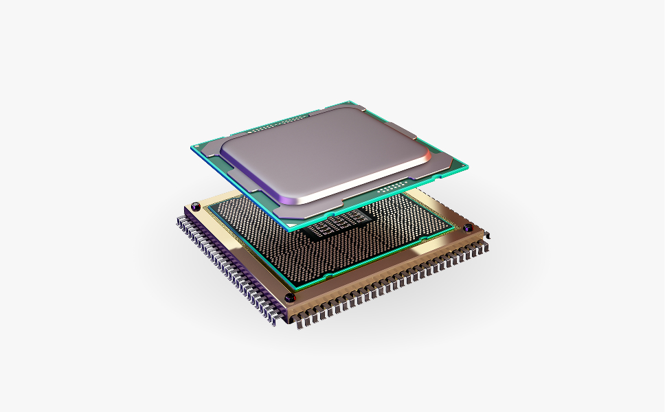
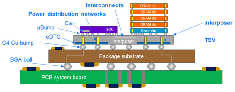
The advanced packaging technology (APT) is a technology which integrates multiple chips into one package using 2.5D die-to-die interconnections such as silicon interposer, redistribution layers (RDL) and 3D die-on-die stacking. It can achieve high performance, low power and smaller form factor for AI, HPC, Networking and ADAS applications.
GUC Solutions

GUC APT Platform
GUC provides a comprehensive solution for advanced packaging, from interposer/RDL design, SI/PI/Thermal simulations, IP, package and substrate design, to high-volume production. Our expert team is well-experienced in the most cutting-edge advanced packaging technologies.
GUC Solutions

System Simulation
Chip-Package-PCB co-design and co-simulation sign-off are critical to advanced products for performance and reliability, especially 2.5D/3DIC integration. GUC in-house solution includes electrical signal & power integrity, power distribution networks (PDN), system thermal integrity and mechanical warpage and stress co-simulation. Product performance is enhanced through floorplan, physical designs, bump/ball assignments, I/O signals break-outs and timing budgets optimization.
GUC Solutions
Total Solution of Signal/Power Integrity & Advance Packaging Design
- HBM and UCIe high speed interconnect design
- Chip, interposer, package and board Power-aware signal Integrity co-optimization
- Si proven with good electrical design margin and eye diagram correlation
GUC Solutions
Whole System Power Integrity
4. SoC core power whole system PDNs IR-drop and Ldi/dt co-design & sign-off
5. Power distribution networks (PDNs) budgeting design & on-/off-chip decap co-optimization
6. Voltage fluctuation & droops co-simulation and Vpeak-peak & Vmin characterization
GUC Solutions
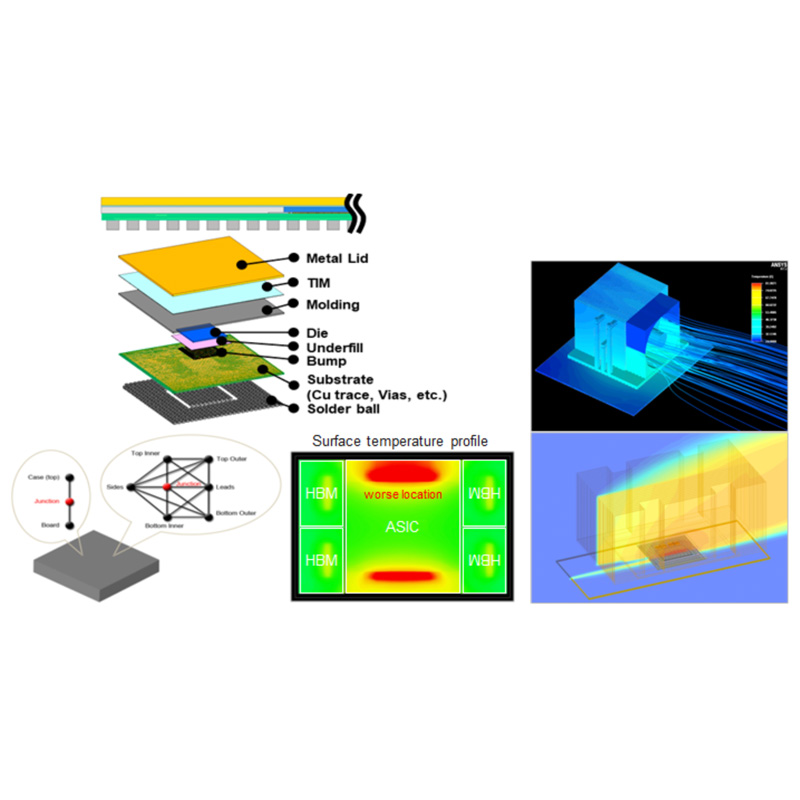
Packaging & System Thermal Integrity - 2D/2.5D/3D-IC Design
7. Early & sign-off stage thermal assessment with chip /chiplet /package /system co-optimization
8. Thermal resistance parameter modeling for multiple packaging topology design & decision
9. Compact thermal models generation and system-level thermal /cooling co-development
GUC Solutions
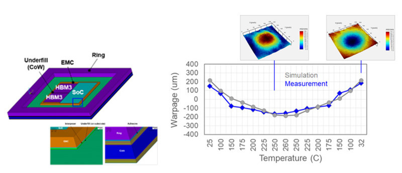
Packaging Mechanical Warpage & Stress - 2D/2.5D/3D-IC Design
10. Early & sign-off-stage mechanical simulation for different packaging solutions
11 . Mechanical warpage & stress risks assessment and chiplets floor-planning integration
12. Package design analysis with mechanical-aware co-optimization, e.g., BoM, layer stacks
13. Mechanical stress analyses for package routability and physical design co-optimization
GUC Solutions
GUC APT IP Portfolio
GUC APT IP has been well recognized by customers and industry. These award-winning IPs mark our leading position in APT. We also provide IP customization alone with our turn-key ASIC design service to our APT customers.
Timeline of GUC APT Flow
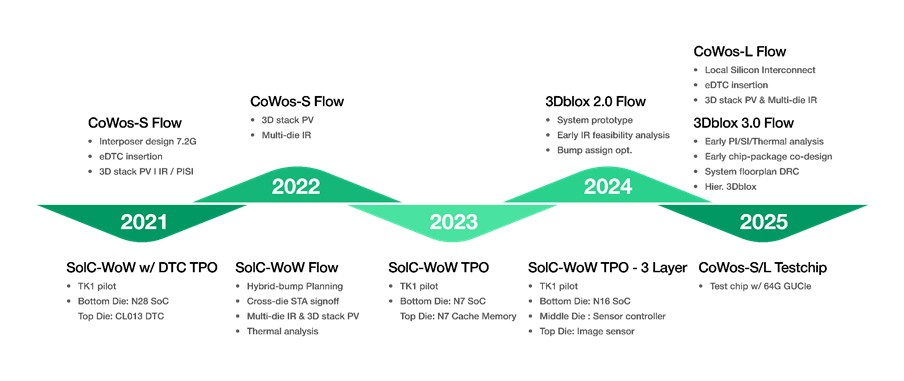
GUC is a pioneer in the development of advanced packaging technology.
In 2016, GUC developed our first HBM (High Bandwidth Memory) IP in TSMC 16nm FinFET process and CoWoS (Chip-on-Wafer-on-Substrate) technology. In 2018, we delivered the first 16nm CoWoS customer product which integrates four HBM2 chips and high-speed SerDes interface for AI applications.
Our APT flow is reliable and up-to-date. It’s well-proven by our APT IP, in-house testchips, and leading customer products.