Information
Package Design Service
Package and Substrate Layout Design
Leading provider of advanced package solutions, specializing in complex and cutting-edge packaging design solutions. GUC’s package design capabilities cover a wide range of package types and advanced technologies, including:
- Expertise in 2.5D (CoWoS & InFO_oS) and 3D (SoIC) packaging to achieve higher integration density and performance enhancement
- Proficiency in SIP (system in package), MCM (Multi-Chip-Modules), Flip-Chip and FCCSP package designs to meet the requirements of high-performance applications.
- Provide lead-frame based package such as QFN, QFP, etc. for cost competitive solutions
Package and Substrate Layout Design

Excellent in-house package and substrate layout design capabilities, providing cutting-edge solutions to meet the needs of advanced packages.
- Advanced package design and feasibility evaluation.
- Choosing optimal package and substrate materials to meet performance, thermal and cost requirement.
- Substrate layer stack-up optimization for performance, cost, and manufacturability balance
- Optimizing substrate design for signal and power integrity
- Optimizing substrates to efficient heat dissipation
- High-density layout connections and ball assignments to enable compact designs with high I/O density and reduce package size
System Simulation

Chip-Package-PCB co-design and co-simulation sign-off are critical to advanced products for performance and reliability, especially 2.5D/3DIC integration. GUC in-house solution includes electrical signal & power integrity, power distribution networks (PDN), system thermal integrity and mechanical warpage and stress co-simulation. Product performance is enhanced through floorplan, physical designs, bump/ball assignments, I/O signals break-outs and timing budgets optimization.
Total Solution of Signal/Power Integrity & Advance Packaging Design

- HBM and UCIe high speed interconnect design
- Chip, interposer, package and board Power-aware signal Integrity co-optimization
- Si proven with good electrical design margin and eyediagram correlation
Whole System Power Integrity
- SoC core power whole system PDNs IR-drop and Ldi/dt co-design & sign-off
- Power distribution networks (PDNs) budgeting design & on-/off-chip decap co-optimization
- Voltage fluctuation & droops co-simulation and Vpeak-peak & Vmin characterization

Packaging & System Thermal Integrity - 2D/2.5D/3D-IC Design
- Early & sign-off stage thermal assessment with chip /chiplet /package /system co-optimization
- Thermal resistance parameter modeling for multiple packaging topology design & decision
- Compact thermal models generation and system-level thermal /cooling co-development

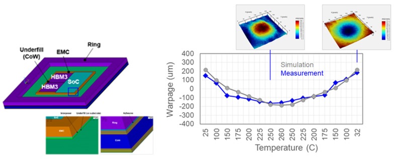
Packaging Mechanical Warpage & Stress - 2D/2.5D/3D-IC Design
- Mechanical warpage & stress risks assessment and chiplets floor-planning integration
- Package design analysis with mechanical-aware co-optimization, e.g., BoM, layer stacks
- Mechanical stress analyses for package routability and physical design co-optimization