HSINCHU, Taiwan — Sep. 22nd, 2026 — Global Unichip Corp. (GUC), the Advanced
ASIC Leader, today announced that its HBM4E PHY and Controller IP is design-ready
and has been adopted in customer AI ASICs. Implemented on TSMC's cutting-edge
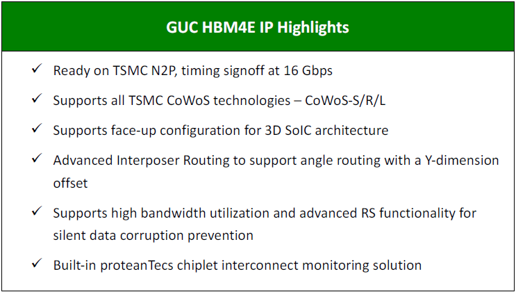
N2P process, the HBM4E PHY has successfully taped out on TSMC CoWoS®-L
advanced packaging technology.
Building on GUC's silicon-proven 12 Gbps HBM4 IP on TSMC's N3P process, the new
HBM4E IP pushes data transfer speeds up to 16 Gbps across all signed-off operating
conditions while delivering industry-leading power efficiency and an ultra-compact
area footprint. Leveraging GUC's proprietary interposer layout technology, the IP is
fully optimized for signal integrity (SI) and power integrity (PI) across various TSMC
CoWoS packaging configurations.
To power 3D SoIC architectures, GUC's HBM4E IP includes a face-up variant
engineered for use as a bottom die in TSMC SoIC®-X technology. It integrates
dedicated Through-Silicon Vias (TSVs) for signal pull-out and feedthrough power
delivery to top dies, establishing a seamless path for complex 3D integration.
In line with GUC's proven HBM, GLink, and UCIe portfolios, the HBM4E IP
incorporates proteanTecs’ interconnect monitoring technology. This integration
enhances visibility during PHY testing and characterization while maximizing in-field
performance and system reliability.
“HBM4E marks a major leap forward in bandwidth and system-level performance for
next-generation AI accelerators. Reaching 16 Gbps on TSMC's N2P process
underscores GUC's ability to quickly turn leading-edge process and packaging
technology into production-ready HBM solutions,” said Igor Elkanovich, CTO of GUC.
“By uniting our face-up HBM, face-up UCIe, and GLink-3D IPs, GUC delivers a
complete interface IP portfolio for 3D SoIC architectures — the foundation for
modern AI ASICs—enabling customers to seamlessly connect HBM, chiplets, and 3D
dies that leverage the most advanced process technology.”