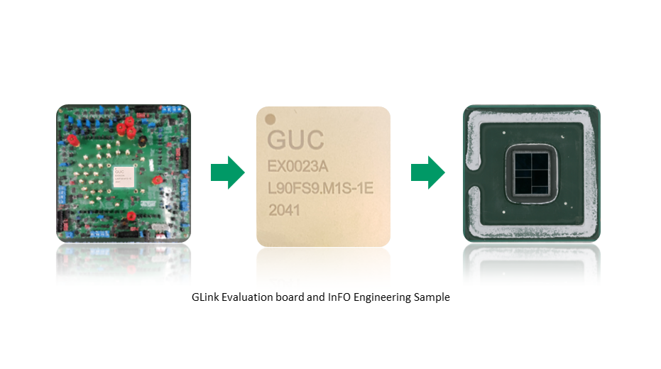
Silicon Proven GLink D2D Solution Using TSMC 7nm Process and 2.5D InFO
GUC Successfully Demonstrates GLink Die to Die Interface IP using TSMC 7nm Process and InFO Advanced Packaging Technology for AI, HPC and Networking applications to do multi-die integration for system scaling.
- Error-free Link, full duplex 0.7 Tbps traffic per 1 mm of beachfront
- 0.25 pJ/bit (i.e., 0.25W per 1 Tbps of full duplex traffic)
- Testing results fully correlated with pre-silicon simulations in all PVT corners
- PPA advantage over SerDes/Package Substrate
6 to 10 times lower power consumption.
For every 10 Tbps of full duplex traffic it consumes 15 to 20 W less
Twice less silicon area.
- GLink over CoWoS is adopted by customers using multi-die ASICs with HBM memories.
- GLink over InFO_oS is adopted due to InFO_oS cost efficiency for modular, scalable and high-yield multi-die ASICs.
- GLink’s low area/power overhead for high throughput interconnect enables efficient multi-die CoWoS and InFO_oS solutions up to 2500mm2.
Read More
GUC 核心优势
- Advanced Packaging Technology Leadership
- Design Engineering Excellence
- Customer Trusted Service