GUC packaging service provides product package evaluation, package design, substrate layout and complete electrical and thermal simulation to ensure product can meet system performance specification.
Package Design
MCM & SiP Package
- GUC has more than 50 projects with multi-chip package in production, including SiP, MCM, MPM and APT (advanced package technology)
- Complete KGD selection and management methodology
- Comprehensive co-design flow to integrate KGD, ASIC, Package and PCB
- In house substrate design and layout: quickly assess D2D connectivity feasibility and I/O fanout optimization
- Electrical simulation: Expertise in SI/PI methodology to achieve design required electrical performance
- Thermal simulation: thermal resistance parameter, high power package, heat sink analysis, and thermal models to support system thermal solutions
Diversified SiP/MPM/MCM Configuration
MPMFCBGA
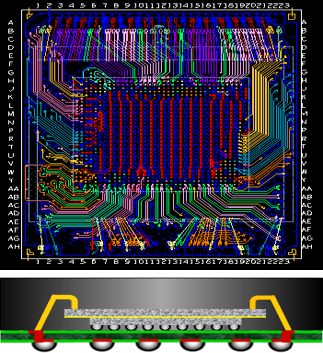
1 SoC+ 8 FCRAM
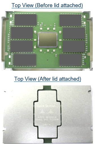
- Package size: 55x72mm2
- Substrate layer: 4-2-4 L
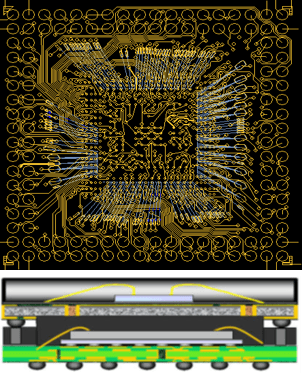
MPMFCBGA
1 SoC + 2 LPDDR
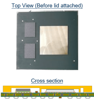
- Package size: 57.5x57.5mm2
- Substrate layer: 8-2-8 L
- Metal TiM for thermal enhancement
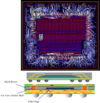
MCMFCBGA
2 SoC
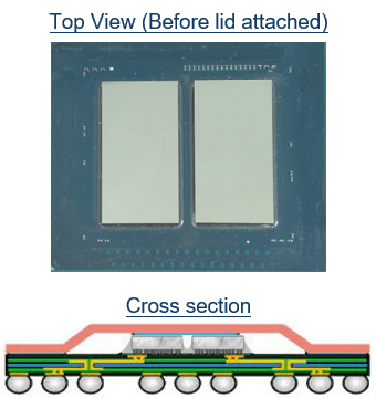
- Package size: 45x45mm2
- Substrate layer: 5-2-5 L
SiP: MCM
SoC+SDRAM+Flash
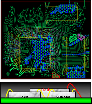
- MCMTFBGA 10x10 mm2
SiP: Hybrid
SoC+LPDDR2/3
- Hybrid, 10x12 mm2
SiP: PoP
MEM+SiP(DBB+PMIC)
- POPFCBGA, 12x12 mm2
SiP: MCeP PoP
HBW MEM+AP
- MCeP POP, 15.7 x 15.7 mm2
- Top Mem: 14 x 14 mm2
Advanced Package
Delivered 1st CoWoS product with 56Gbps SerDes package solution in 2018. Working on InFO_oS for mutli-chips high-speed interconnection solution.
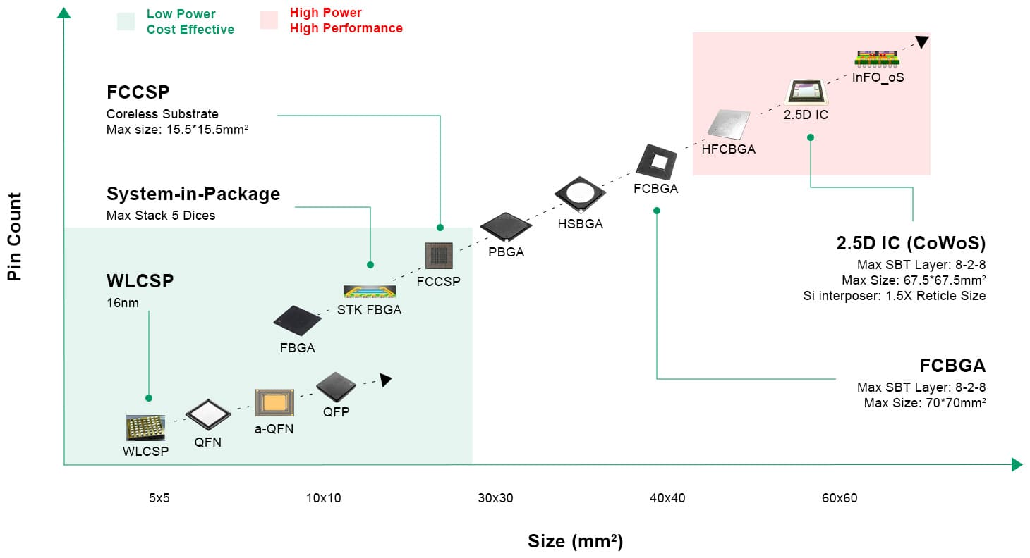
2.5D IC Packaging
2.5D IC packaging technology integrates multiple chips into one package enables product higher performance, lower power consumption and smaller form factor for the advanced products targeting AI and HPC applications. It also supports advanced technology node Si yield and cost saving via die partitioning and multi-core expansion.
In 2016, GUC adopted TSMC's advanced CoWoS (Chip-on-Wafer-on-Substrate) packaging technology for our first HBM (High Bandwidth Memory) IP by TSMC 16nm FinFET process and successfully validated 65nm interposer design, DFT, package and test solutions. In 2018, the first 16nm CoWoS real product was delivered integrating four HBM2 chips with high-speed SerDes interface for AI applications. After that, GUC has completed many CoWoS products design in 7nm and continuously been developing our 5nm/3nm IP to support the advanced products with higher bandwidth HBM2E/HBM3 integration.
Chip-Package-Board Co-Simulation
- Chip-Package-Board co-design and co-simulation are critical to high speed products for performance enhancement by optimizing floor plan, layout, pad location, I/O and electrical timing budgeting among chip, package and board. GUC’s co-simulation includes mechanical, electrical signal integrity and power integrity and thermal performance.
- Achieve cost effectiveness by identifying optimized package configuration and size and substrate layers.
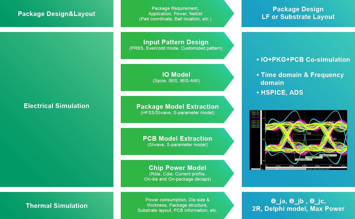
CoWoS Chip-Interposer-Package-Board Electrical and Thermal Co-simulation
- Perform whole system level power distribution network co-simulation. Extract all interconnect channel effect into co-simulation database, including TSV, via, interposer trace, PTH, package, PCB trace, ubump, C4 bump, BGA ball, decap, etc.
- Through electrical co-simulation to optimize package decap combination for voltage drop and variation improvement.
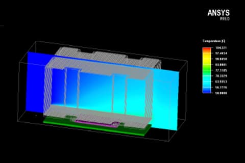
- Thermal simulation model base on real geometry and material property. It is able to support package/interposer modeling and package/system thermal analysis to optimize the system performance.
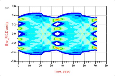
Signal Integrity Co-simulation
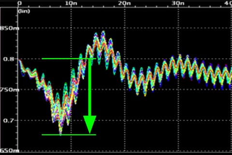
Power Integrity Co-simulation
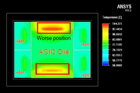
System Level Thermal Co-simulation
Another TSMC advanced packaging technology InFO_oS (Integrated Fan-Out on Substrate) features high density RDL to integrate multiple advanced logic chiplets for networking application. In 2020, GUC also developed the first GLink IP for die-to-die connection by TSMC 7nm/6nm technology to support the most advanced products design. It's expected more and more InFO_oS adoption with die-to-die connection solution to integrate chiplets for the next generation products.