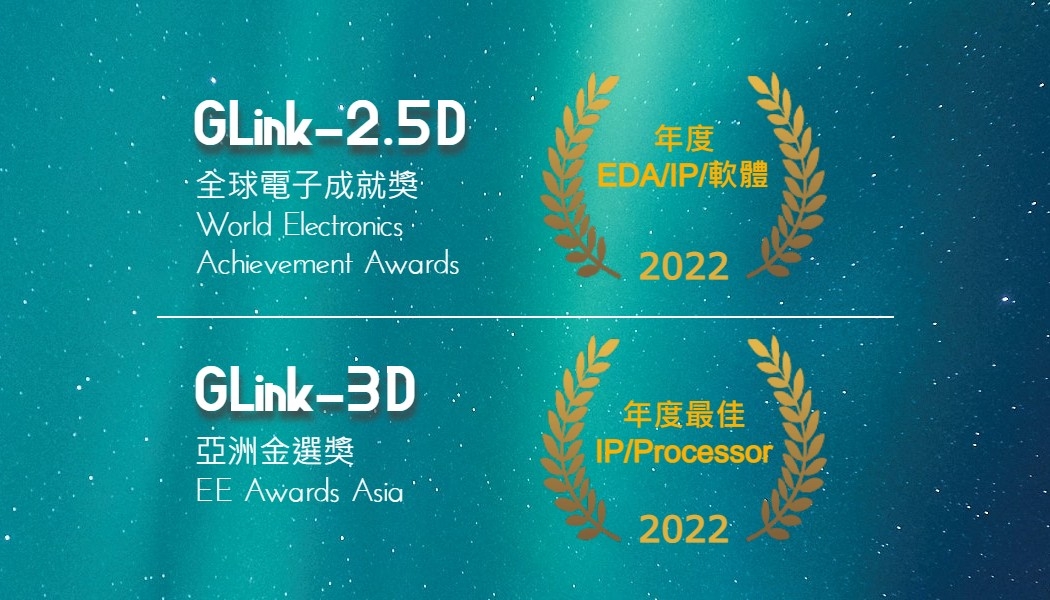
GUC GLink Received Awards in China (Nov/10) and Taiwan (Dec/08)
We’re honored that GLink received two awards this year as recognition of our technology, innovation, and expertise.
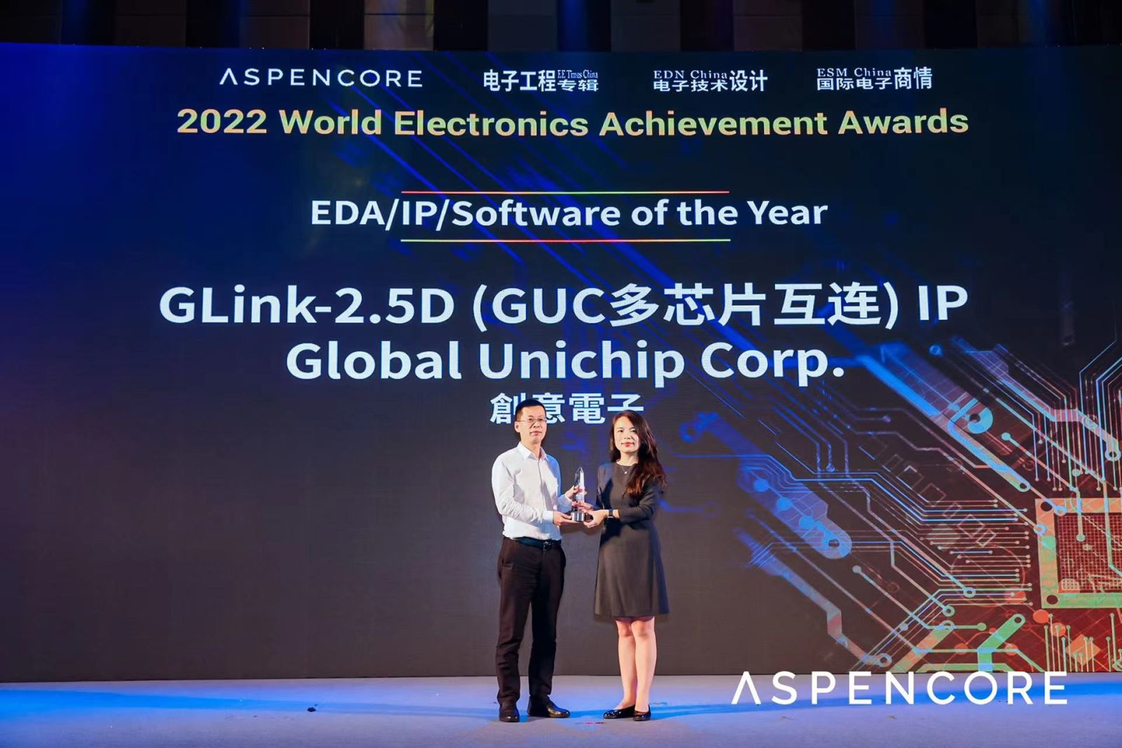
- GLink-2.5D : World Electronics Achievement Awards – EDA/IP/Software of the Year
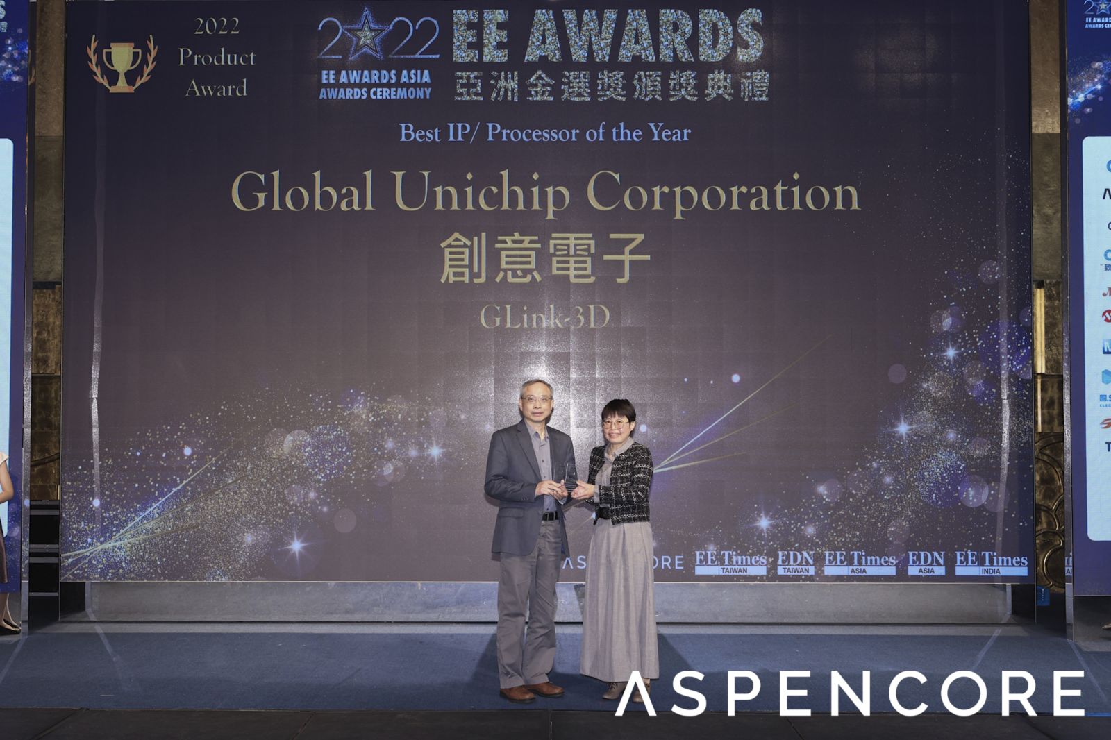
- GLink-3D : EE Awards Asia – Best IP/Processor
Die edge is the scarcest resource and GLink-2.5D allows the most efficient use of it by transferring 2.5 Tbps of full duplex user traffic per every mm of die edge. With end-to-end latency of 5 ns and measured power consumption of 0.27 pJ/bit, this is the most efficient chiplet interface on the market. GLink-2.5D supports InFO_oS and all CoWoS types (both silicon –S and organic interposers -R). Leading AI, CPU and Automotive customers have adopted it for their next generation products.
GUC GLink-3D IP family provides high speed die-on-die interface Master PHY and Slave PHY. They are used to transmit data between dies, assembled using TSMC System on Integrated Chips (SoIC) 3D stacking technology (3DFabric). The IP supports both Wafer-on-wafer (WoW) and Chip-on-wafer (CoW) assembly, both face to face and face to back options. Both Master and Slave PHY are built of TX and RX Data and Command Slices in a modular way, used to communicate between dies with high data bandwidth and low end-to-end latency, data rate per bond up to 5.0 Gbps. Other major valuable advantages include easy to converge cross-die timing closure for huge amount of high speed signals, and embedded data training, DFT and repair functions to achieve high multi-die yield.
Learn More: https://www.guc-asic.com/en/solution-ip-d2d.php
For more information, please contact your GUC sales representative directly or email guc_sales@guc-asic.com
GUC 核心优势
- Advanced Packaging Technology Leadership
- Design Engineering Excellence
- Customer Trusted Service