GLink-3D IP has been taped out in Apr'21 using TSMC 3DFabric Technology and granted by the U.S. patent in Jun'21
Logic circuit gains higher density and performance when scaled to N5/N3 process nodes but SRAM scaling from N7 to N5/N3 is moderate. SRAM/Logic disintegration allows to implement separate SRAM and Logic at the most efficient process nodes. Layers of CPU and SRAM (Last Level Cache, packet buffers) dies can be assembled over and under interconnect/IO dies using TSMC 3DFabric technology. Such expandable SRAM and modular compute applications are enabled by GUC GLink-3D high bandwidth, low latency, low power, and point-to-multipoint interface between 3D stacked dies. Moreover, the U.S. patent office has granted GUC the patent in Jun'21.
GUC GLink-3D key features:
- Supports 3DIC stacking of combination of N5 and N6 process nodes
- Point-to-multipoint interface allows main die to interface several stacked dies simultaneously
- Robust, full duplex 9.0 Tbps traffic per 1 mm2
- Speed: 5.0 Gbps per lane
- Extremely low end-to-end latency (< 2ns) with low power design (< 0.2 pJ/bit)
- Single supply voltage 0.75V ± 10%
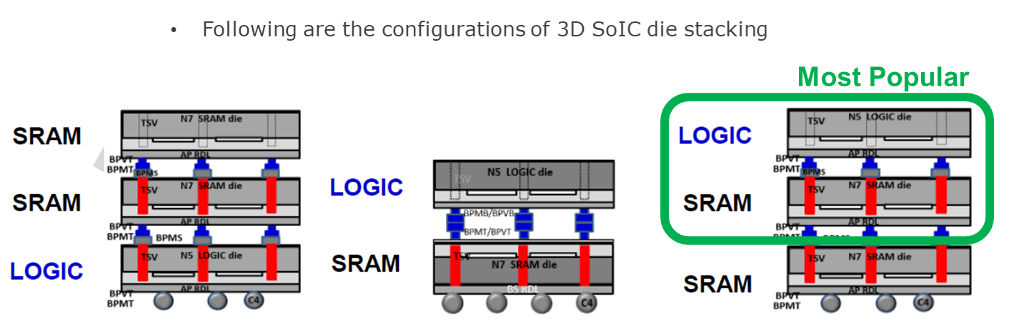
- Supports both face-to-face and face-to-back die stacking
GUC 核心優勢
- Advanced Packaging Technology Leadership
- Design Engineering Excellence
- Customer Trusted Service