GUC Taped Out UCIe 32G IP using TSMC's 3nm and CoWoS Technology
News Content:
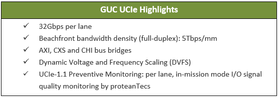
Hsinchu, Taiwan – Jan. 10, 2024 —Global Unichip Corp. (GUC), the Advanced ASIC Leader, announced today that it has successfully taped out Universal Chiplet Interconnect Express™ (UCIe™) PHY IP with 32Gbps per lane, the highest UCIe speed, for AI/HPC/xPU/Networking applications. UCIe 32G chiplet interface provides industry leading bandwidth density 10 Tbps per 1mm of die edge (5 Tbps/mm full-duplex). The chip uses TSMC’s N3P silicon process and CoWoS® advanced packaging technology.
In recent years GUC has developed a family of chiplet interconnect IPs (GLink-2.5D) in TSMC N7, N5 and N3 process nodes. GLink-2.5D IPs were validated in silicon demonstrating robust operation up to 17.2 Gbps with raw BER<1E-20. Built-in CRC checkers and retransmit buffers allowed to achieve <<1 FIT, meeting the strictest automotive reliability requirements. GLink-2.5D supports full range of TSMC 2.5D technologies (CoWoS-S/R/L, InFO_oS).
The UCIe Consortium has set a vision of interoperability of chiplet interfaces. GUC's implementation of UCIe takes advantage of many silicon-proven generations of GLink-2.5D IPs, making the lowest risk path to UCIe with the highest performance parameters. GUC also developed bridges for AXI, CXS and CHI buses using UCIe Streaming Protocol. These bridges are optimized for high traffic density, low power, low data transfer latency and efficient end-to-end flow control, facilitating seamless transition from single chip NoC to chiplets architecture. The bridges support Dynamic Voltage and Frequency Scaling (DVFS) allowing voltage and bus frequency change on the fly while ensuring uninterrupted data flow.
GUC’s UCIe IP supports UCIe-1.1 Preventive Monitoring functionality. It includes proteanTecs’ I/O signal quality monitors which were already tested in GLink-2.5D family. Signal quality is monitored in mission mode, during data transfer, without re-training or causing any data transfer interruption. Every signal lane is continuously monitored and reported separately, and power and signal integrity events are detected. Bumps and traces defects are identified before they cause the interface to fail. Repair algorithm then replaces marginal lanes- with redundant ones to prevent system operation failure, so chip lifetime is extended.
“We are proud to announce the world’s first UCIe IP supporting 32 Gbps,” said Aditya Raina, CMO of GUC. “We have established a complete silicon-proven 2.5D/3D chiplet IP portfolio at TSMC’s 7nm, 5nm and 3nm technologies. Together with design expertise, package design, electrical and thermal simulations, DFT and production testing for the TSMC 3DFabric offerings including CoWoS, InFO, and SoIC, we provide our customers with a robust and comprehensive solution, enabling fast design cycles and quick bring up of their AI/HPC/xPU/Networking products.”
“We are committed to delivering the fastest and the lowest power 2.5D/3D chiplets and HBM interface IPs,” said Igor Elkanovich, CTO of GUC. “Convergence of 2.5D and 3D packaging using HBM3/4, GLink-2.5D/UCIe and GLink-3D interfaces enables highly modular, much bigger than reticle size processors of the future.”
