GUC GLink 2.5D and 3D Presentation to OCP/ODSA Committee
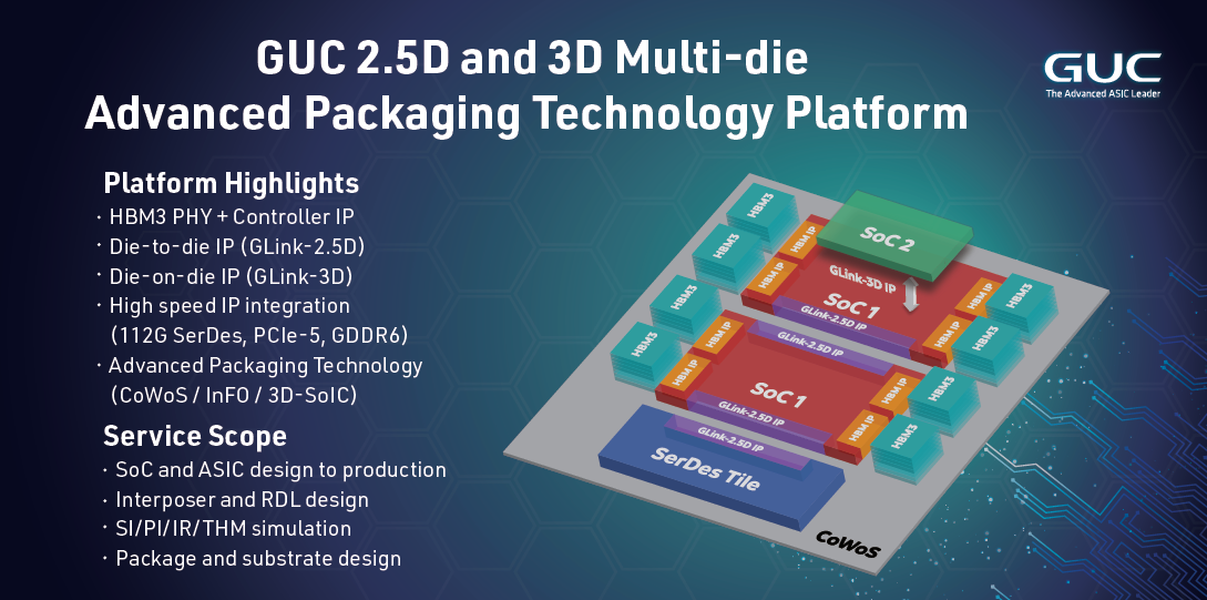
GUC has been developing Die-to-Die and Die-on-Die IP, fully optimized for tsmc advanced packaging technology including 2.5D CoWoS/InFO and 3D SoIC, for many years with full mass production records. For sharing the success experience to industry, GUC CTO Igor Elkanovich gave a speech to OCP/ODSA committee in April to elaborate on technology advance on the latest 2.5D and 3D advanced packaging and how GUC's GUC-2.5D and GUC-3D IPs can be excellently used together with them to provide the premium PPA for multi-die integrations.
- TSMC's 2.5D (CoWoS and InFO_oS) allows side-by-side integration of multiple dies (processors, SRAM, networking, SerDeses, HBM memories) for high performance, modularity and yield.
- Performance-driven processor dies at 3nm, interconnect dies at 5nm and SRAM/Caches at 7nm can be assembled using TSMC's SOIC (Wafer-on-Wafer, Chip-on-Wafer) technology.
- Convergence of 2.5D and 3D packaging technologies using GUC's HBM, GLink-2.5D and GLink-3D interfaces enables highly integrated processors of the future including Serdeses and HBMs with SRAMs and CPUs/Accelerators dies over/under main dies.
GUC Core Strengths
- Advanced Packaging Technology Leadership
- Design Engineering Excellence
- Customer Trusted Service